Lab 2: Multiplexed 7-Segment Display
Introduction
In this lab, a design was implemented on the FPGA to display two numbers 0-F (hex) on a dual seven-segment display using two 4-input DIP switch. One seven-segment SystemVerilog module and 7 FPGA pins was used to drive both halves of the display by implementing time multiplexing. Five singular LEDs also displayed the sum of the two digits displayed on the seven-segment displays in binary.
Design and Testing Methodology
The seven-segment display consists of diodes corresponding to each of the seven segmenets. It was controlled using combinational logic and 4 DIP switches. Each possible combination of switches lights up a different combination of segments, which corresponds to a distinct digit. Since only one seven-segment display can be controlled at a time by a single SystemVerilog module and 7 FPGA pins, the two digits were blinked on and off at a frequency of 4800 Hz, a frequency too high for the human eye to detect.
The on-board high-speed oscillator from the iCE40 UltraPlus primitive library was used to generate a clock signal at 48 MHz. A counter was used to reduce this frequency to 4800 Hz by inverting an output signal every 10,000 clock cycles. At each of the reduced clock cycles, a multiplexer is used to choose which of the seven-segment displays to turn on (by applying power to the common anode or not).
A PNP transistor was used to drive each of the common anodes of the seven-segment display, since the FPGA GPIO pins are incapable of driving sufficient current to power all seven segments.
The output of LED[5:0] corresponds to the sum of the two digits displayed on the seven-segment displays.
The design was developed using four modules: a top module, a for the clock counter, a module for the seven-segment display logic, and a module for the 2:1 multiplexer.
Technical Documentation
The source code for the project can be found in the associated Github repository
Calculations
According to the iCE40 UltraPlus Family Data Sheet section 4.17, the maximum output current for a single FPGA I/O pin (IOL / IOH) is 8 mA. Using a 150 Ω resistor, and with a diode forward voltage of 2.0V, the amount of current draw for a single segment is 8.67 mA, already exceeding the maximum allowable current draw for a pin. Seven segments will require 60.7 mA of current.
To account for this, a PNP transistor can be used to provide enough current for the entire display. The base of the transistor is connected to the FPGA pin in series with a 2.2 kΩ resistor, which limits the current through the pin to 1.1 mA. The emitter is connected to power, and the base is connected in series with the LED segent, a 150 Ω resistor, and an FPGA output pin. The PNP transistor has a DC current gain of 80 for the magnitudes of currents desired, which is plenty large enough for what is required.
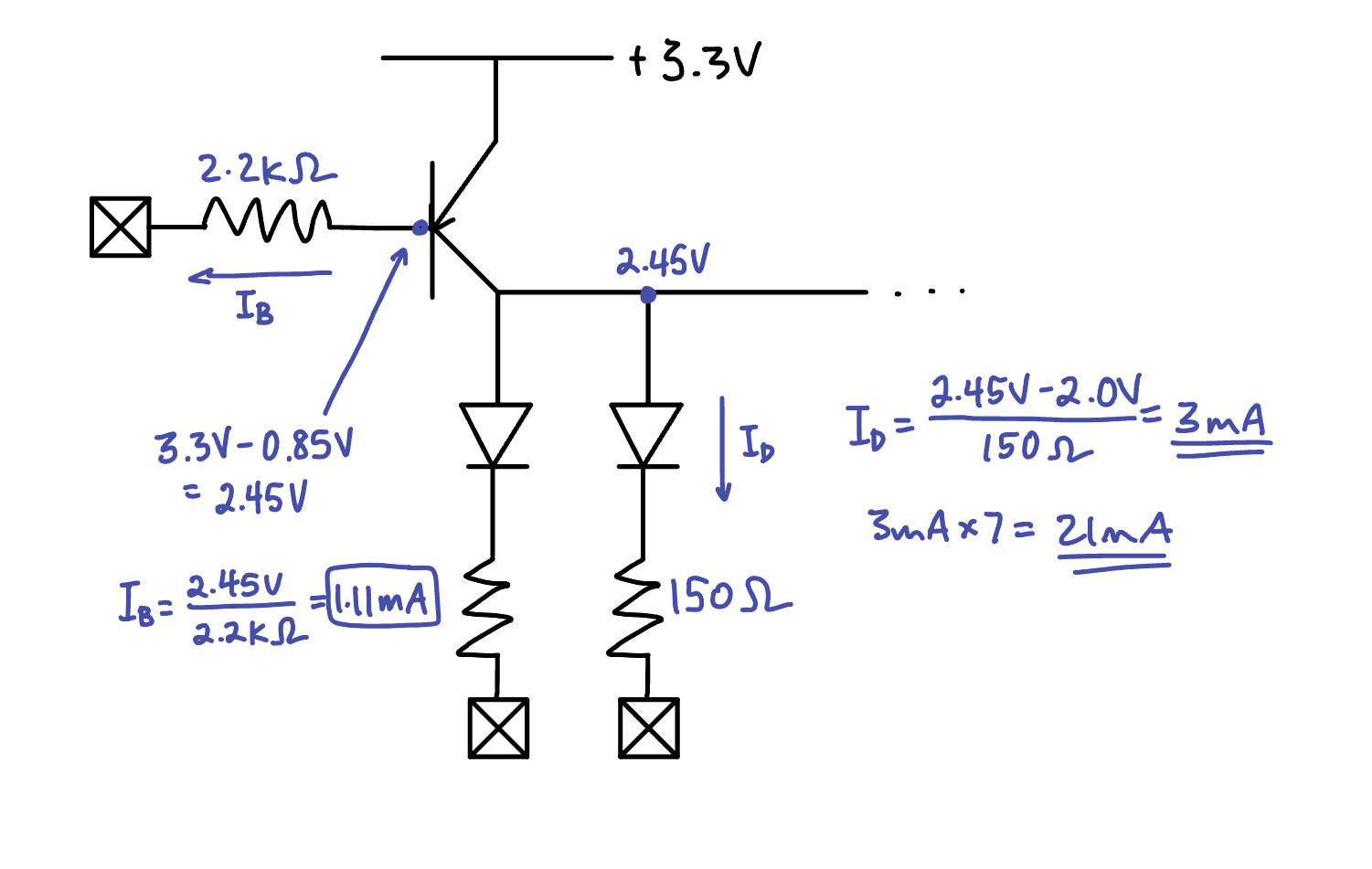 Figure 1: Calculation for current draw through each of the seven segments and the current draw through the FPGA pin when using the transistor.
Block Diagram
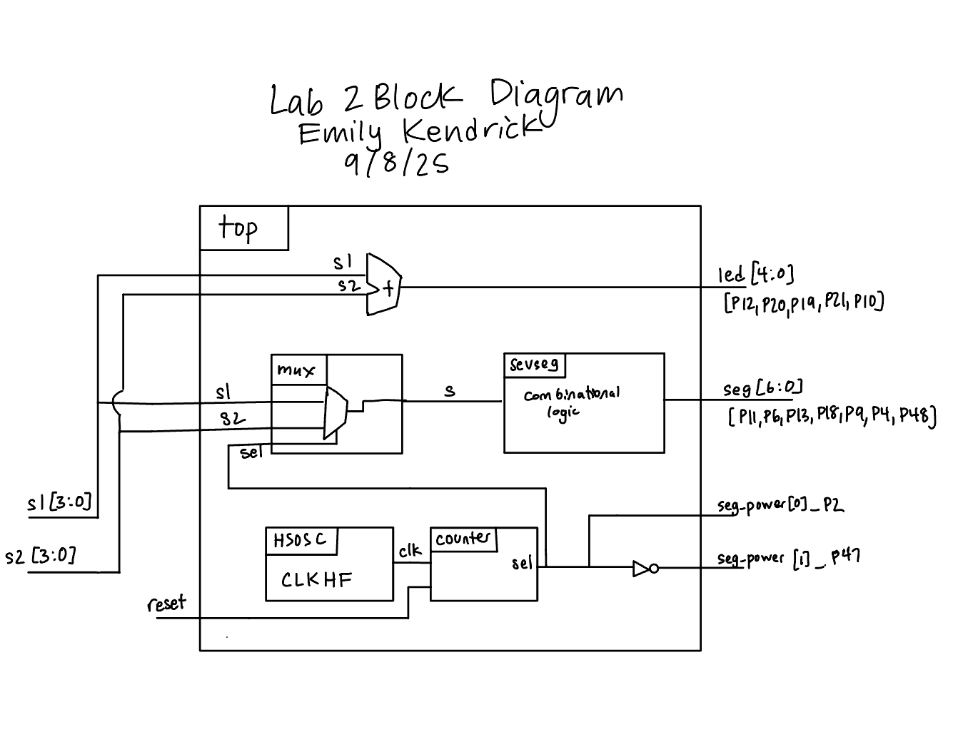 Figure 2: Block diagram
Schematic
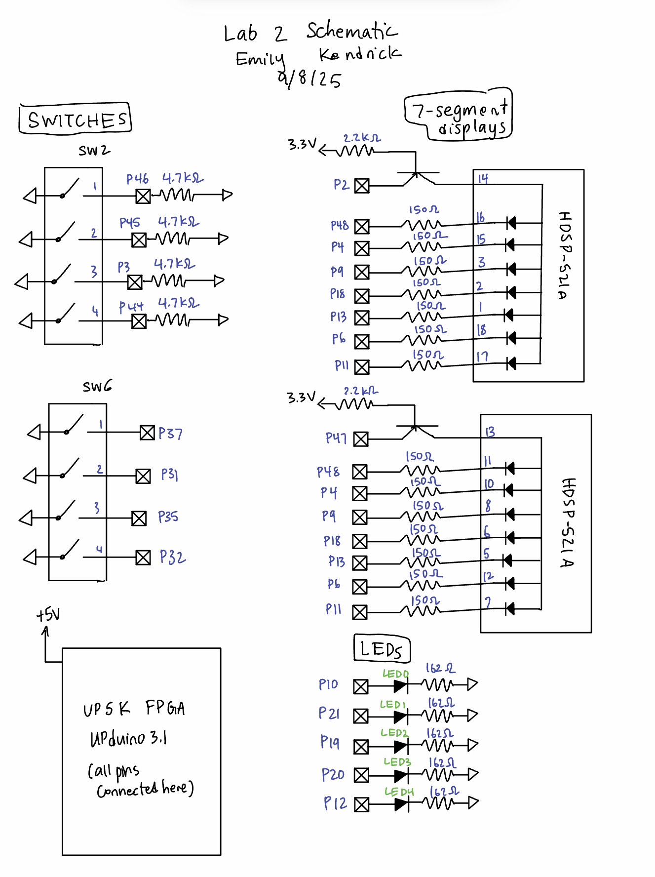 Figure 3: Electrical schematic
Results and Discussion
The design performed as expected. It displayed the two digits without any blinking or bleeding visible to the human eye, and controlled five external LEDs.
Testbench Simulation
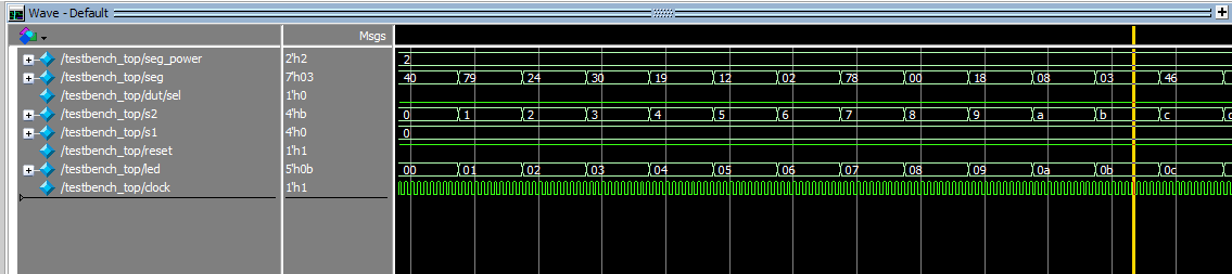
Figure 4: A screenshot of the testbench simulation demonstrating successful running of the top module.
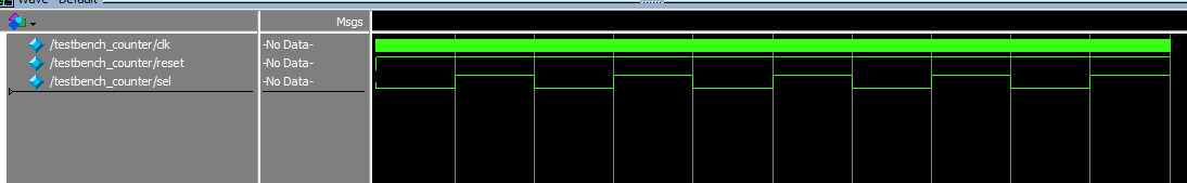
Figure 5: A screenshot of a testbench simluation demonstrating the counter module. The period of the clock was increased from 20 ns to 20000 ns, as expected.
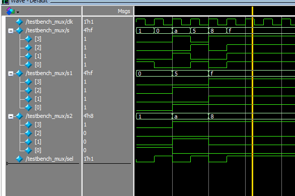
Figure 6: A screenshot of a testbench simulation demonstrating the mux module.

Figure 7: A screenshot of a testbench simulation demonstrating the sevseg module.
The design met all intended objectives.
Conclusion
The design successfully implemented time-multiplexing to blink two seven-segment LEDs using only seven output FPGA pins and a single sevseg module. The LEDs were blinked at a frequency of 4800 Hz. Five other LEDs displayed the sum of the two values displayed on the seven segment displays. I spent 10 hours on this lab.
AI Prototype Summary
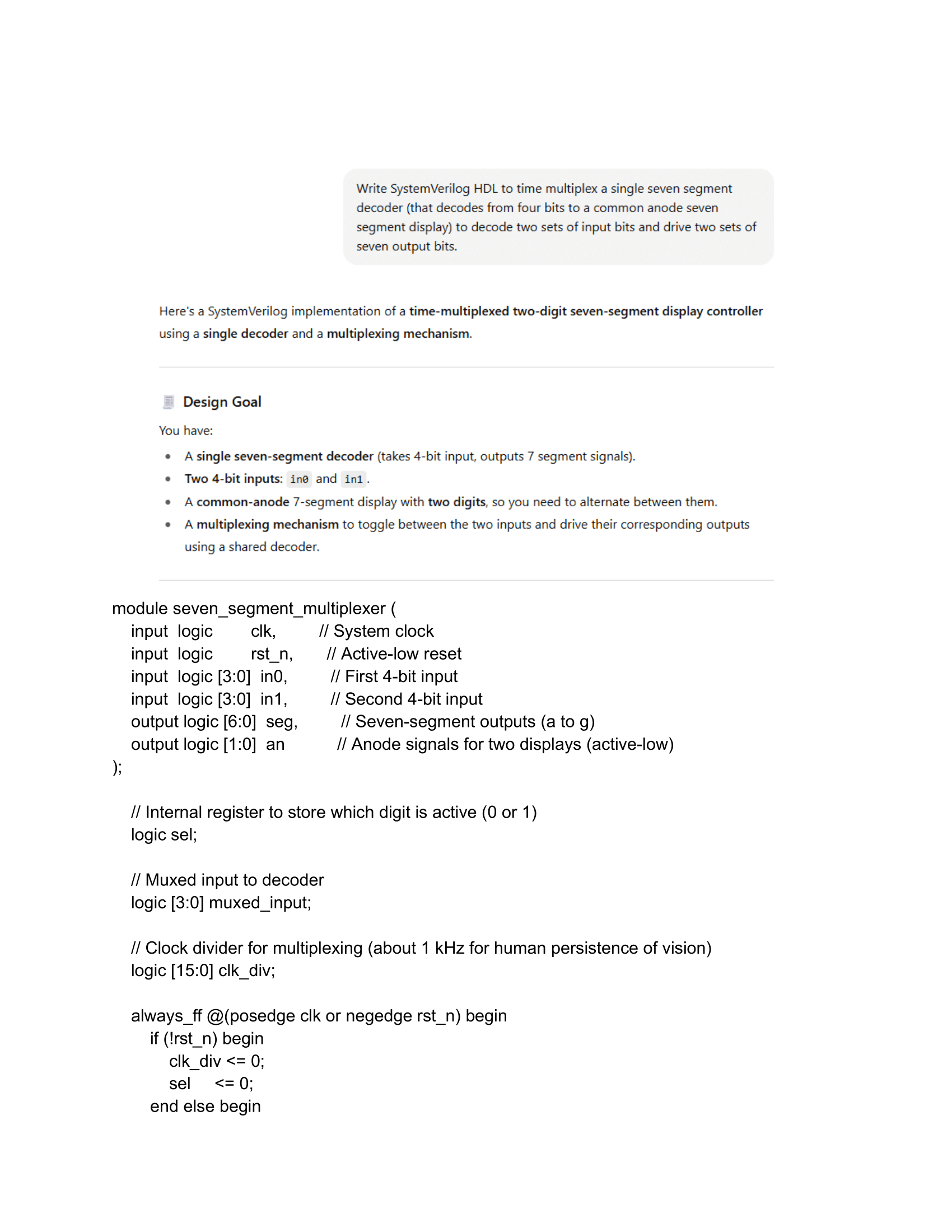
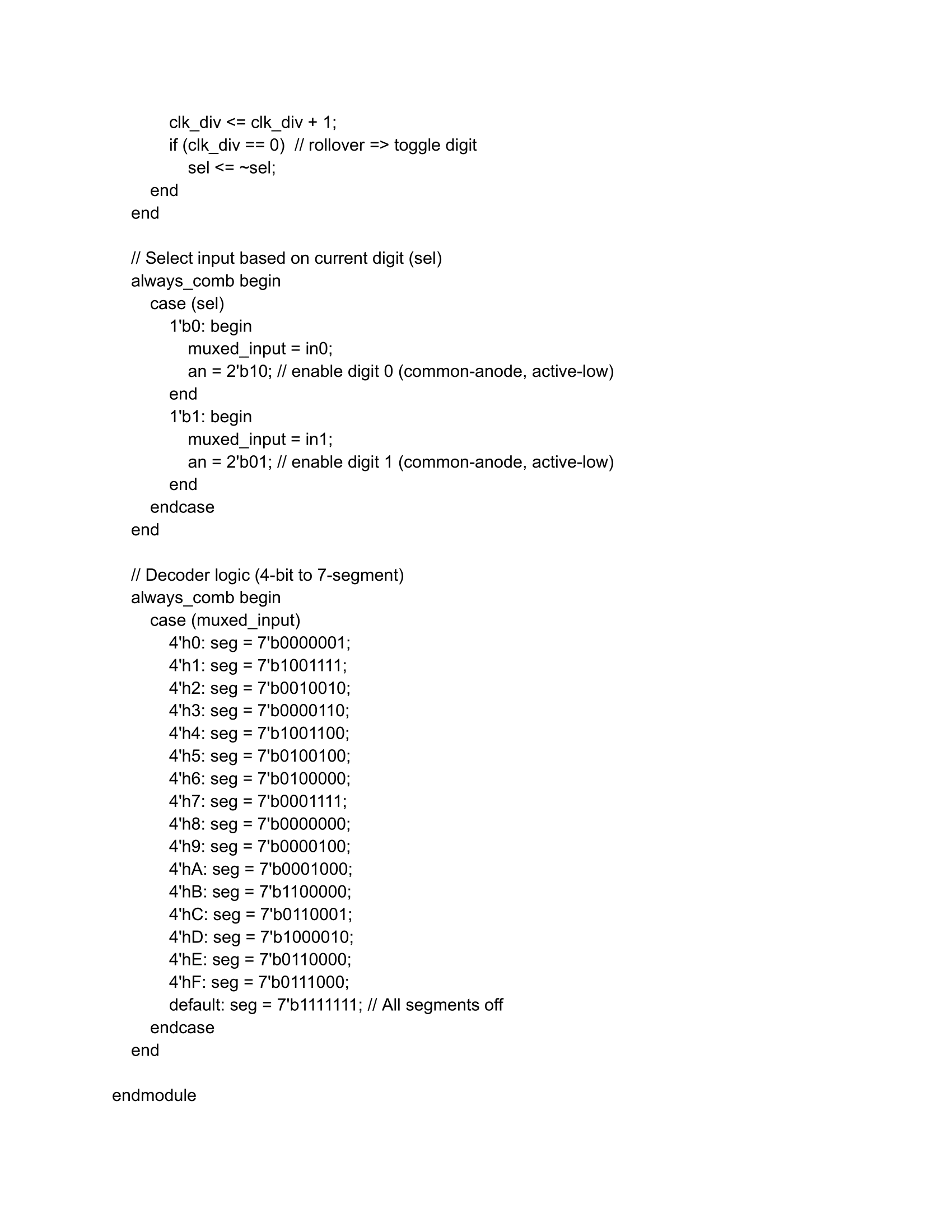
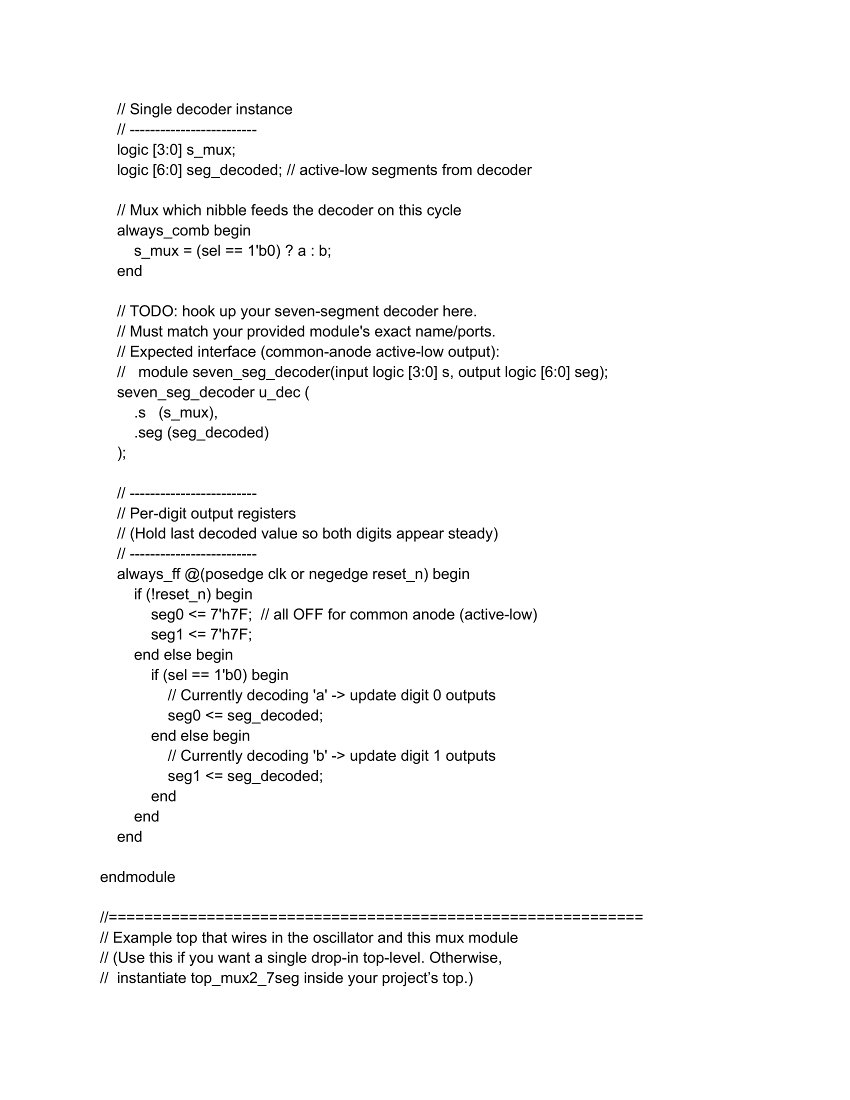
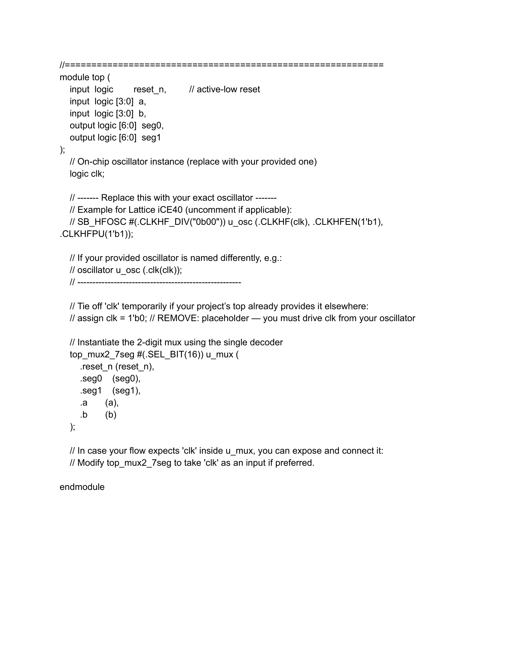
I asked ChatGPT to create a SystemVerilog HDL module to time multiplex a single seven segment decoder to decode two sets of input bits and drive two sets of seven output bits. It created a reasonable script to perform this task, which synthesized on the first try. One thing I noticed is that ChatGPT does not separate functions into seperate modules, and instead leaves everything in a top module, which can make it harder to understand.
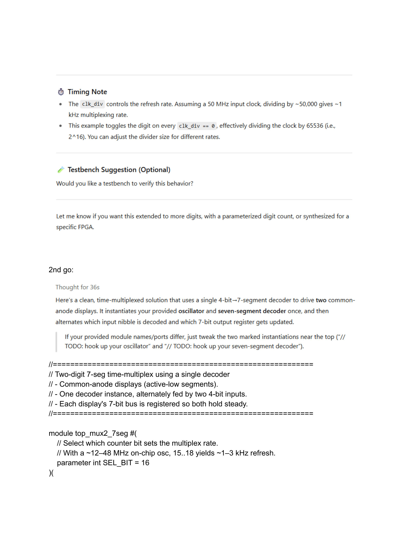
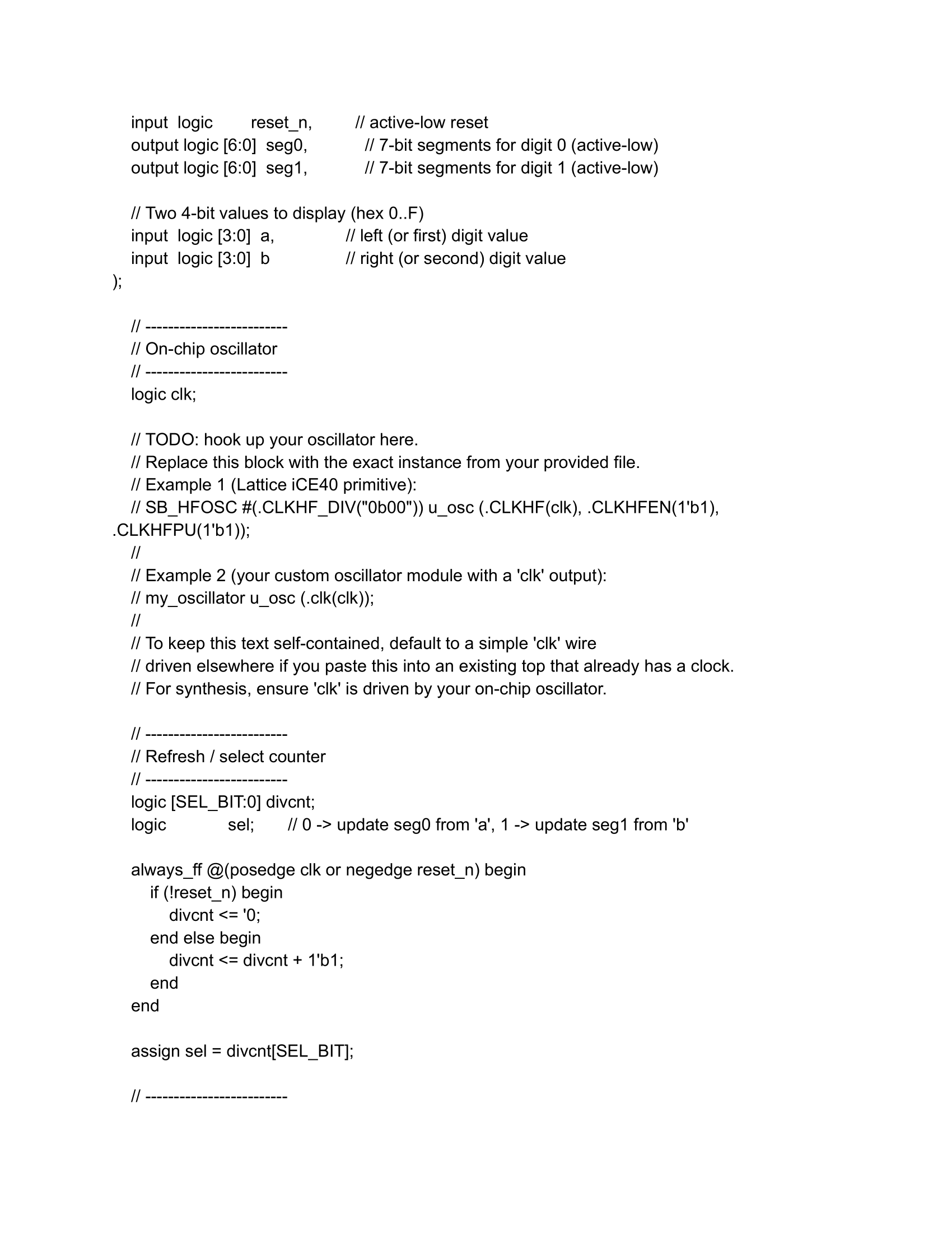
I then asked it to do it again using my files from Lab 1. I don’t think it parsed my files well, because it couldn’t extract the actual name of the module or the clock that I used. The output is shown below: